

Jul 24, 2026
Modern electronic systems continue to increase in power density while package sizes become smaller. As a result, thermal management has become a critical design consideration in power electronics. Circuit protection applications, including battery protection, reverse-current blocking, and bidirectional switching, commonly use common-drain dual MOSFETs. While these devices enable compact and efficient designs, their thermal performance is often limited by PCB layout constraints.
Dual MOSFETs can be implemented using either common-source or common-drain configurations. In many circuit protection applications, the common-drain topology is preferred because it blocks current flow in both directions when the MOSFETs are turned off.
However, this configuration also creates a thermal challenge. The shared drain node is electrically active, preventing the drain-connected copper from being directly connected to a grounded heatsink or ground plane. As power density increases, the available drain-connected copper area is often insufficient to spread the generated heat effectively.
This leads to higher operating temperatures, increased conduction losses, lower system efficiency, and accelerated component ageing. Because MOSFET on-resistance (RDS(on)) increases with temperature, higher device temperatures also increase conduction losses, further reducing thermal performance.
Increasing the copper area connected to the MOSFET is a common way to improve heat spreading. A larger copper area reduces thermal resistance and helps lower device temperature.
In many power electronic designs, however, the size of electrically active copper areas is constrained by electrical and PCB layout requirements. In common-drain dual MOSFETs, this becomes particularly important because the shared drain node is both electrically active and the primary thermal path. While increasing the drain-connected copper can improve heat spreading, it also enlarges the active drain node, making this approach impractical in many compact circuit protection designs.
The challenge is therefore not only to remove heat, but to transfer it efficiently to a larger cooling area without increasing the size of the active drain node.
LTG devices address this challenge by providing an electrically isolated thermal path between the active drain region and a larger grounded copper area.
Rather than increasing the size of the drain-connected copper, LTGs transfer heat to a larger ground plane while maintaining complete electrical isolation. This allows the ground plane to act as an extended heat spreader without changing the electrical architecture of the PCB.
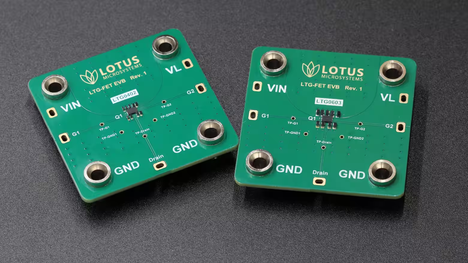
To evaluate this approach, Lotus Microsystems developed evaluation boards using a common-drain dual MOSFET with and without LTG devices. Each board used the same MOSFET, identical operating conditions, and the same circuit topology, allowing the thermal impact of the LTGs to be measured directly.
Two LTG package sizes were evaluated: LTG0402 and LTG0603.
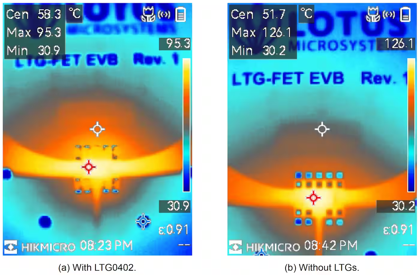
The LTG0402 implementation achieved:
After 15 minutes of continuous operation, the maximum measured surface temperature decreased from 126.1°C to 95.3°C.
The LTG0603 implementation achieved:
After 15 minutes of continuous operation, the maximum measured surface temperature decreased from 124.7°C to 95.2°C.
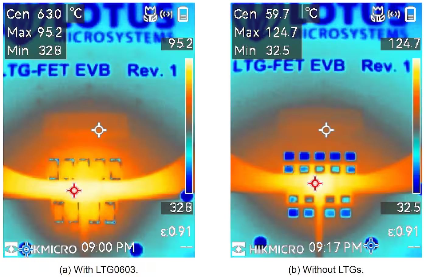
Measurements performed after 5 and 15 minutes of continuous operation showed that the thermal improvement was maintained over time. Together, these results demonstrate that LTG devices provide a substantial and sustained reduction in the maximum measured MOSFET surface temperature.
Thermal management of common-drain dual MOSFETs is fundamentally constrained by the electrically active drain node. While increasing the drain-connected copper area improves heat spreading, it also enlarges the active drain node, making this approach unsuitable for many compact circuit protection designs.
LTG devices overcome this limitation by providing an electrically isolated thermal path to a larger grounded copper area. This enables efficient heat transfer without increasing the size of the active drain node or compromising the electrical design of the PCB.
Experimental testing demonstrated substantial reductions in the maximum measured MOSFET surface temperature. Lower operating temperatures can reduce thermal stress, limit the temperature-dependent increase in RDS(on), improve component reliability and lifetime, and support higher power density in compact power electronics.
Download the application note to explore the evaluation board design, test methodology, and complete experimental results.


