
Lotus Microsystems introduces advanced packaging to the power management field with our proprietary power interposer technology, enabling the use of silicon interposers in power applications. Our interposer design and processes are optimized to handle higher currents and endure higher voltages.
Thick-copper redistribution layer (RDL) patterning
Double-sided wafer routing
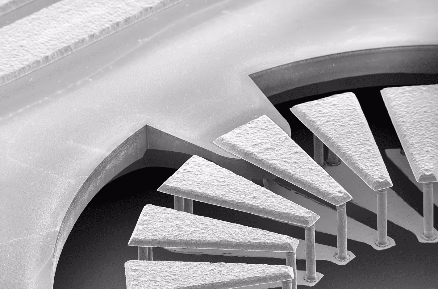
Precision silicon etching
High-aspect ratio through-silicon vias (TSV)
Compared to conventional power module packaging using laminate substrates and lead frames, the Lotus Power Interposer delivers up to 60% better thermal performance while eliminating hot spots. This enables higher power density and reduces derating at the maximum allowable temperature on the application platform.

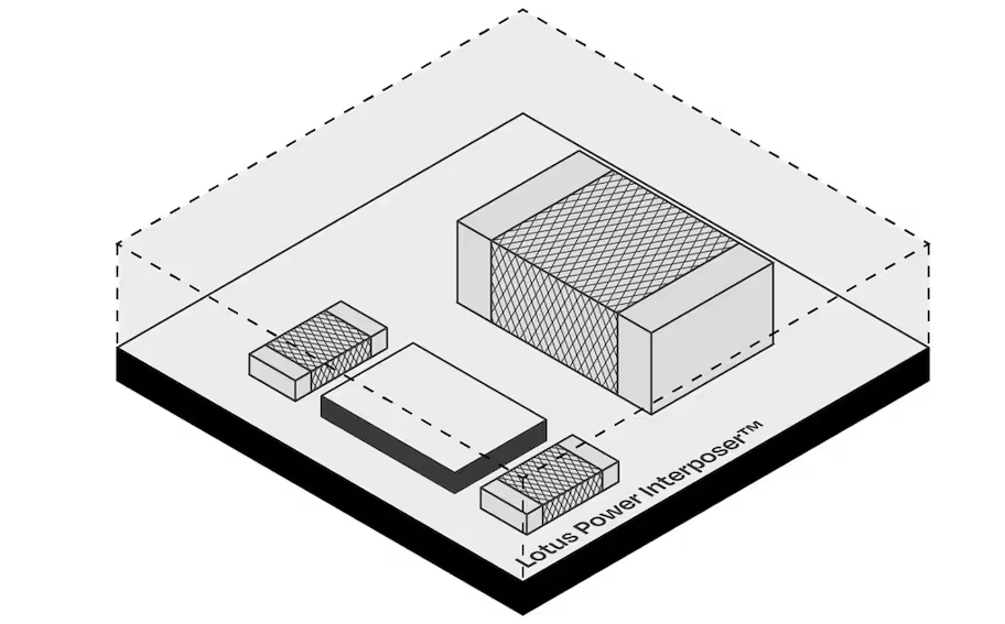
2.5D and 3D packaging for power modules with integrated active and passive components.
Optimized heat distribution of power devices across the substrate in both vertical and lateral paths.
Achieved through lower operating temperatures, minimized parasitics, and an increased allowance for passive components.
Combining multiple technologies, including CMOS, MEMS, GaN, and integrated passive devices (IPDs), into a single package.

