

Oct 19, 2026
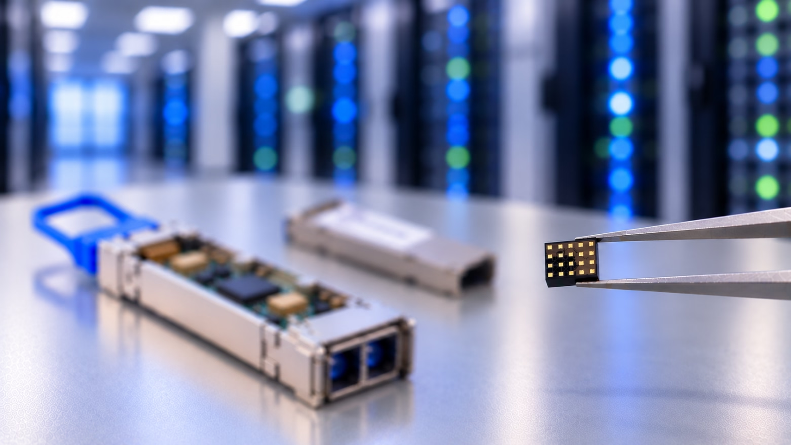
As PCB layouts grow increasingly compact, power supplies are forced to deliver power at >90% efficiency while guaranteeing sub-20 µV RMS noise levels. This is especially needed in optical transceivers, telecom gear, and medical instrumentation where signal integrity is non-negotiable and where footprints are typically under 3 mm × 2 mm.
The LBK0504 by Lotus Microsystems addresses all these requirements with a step-down Power Supply in Package (PSiP) that integrates both the power management IC and the required inductor into a 2 mm × 2.5 mm × 1.1 mm package.
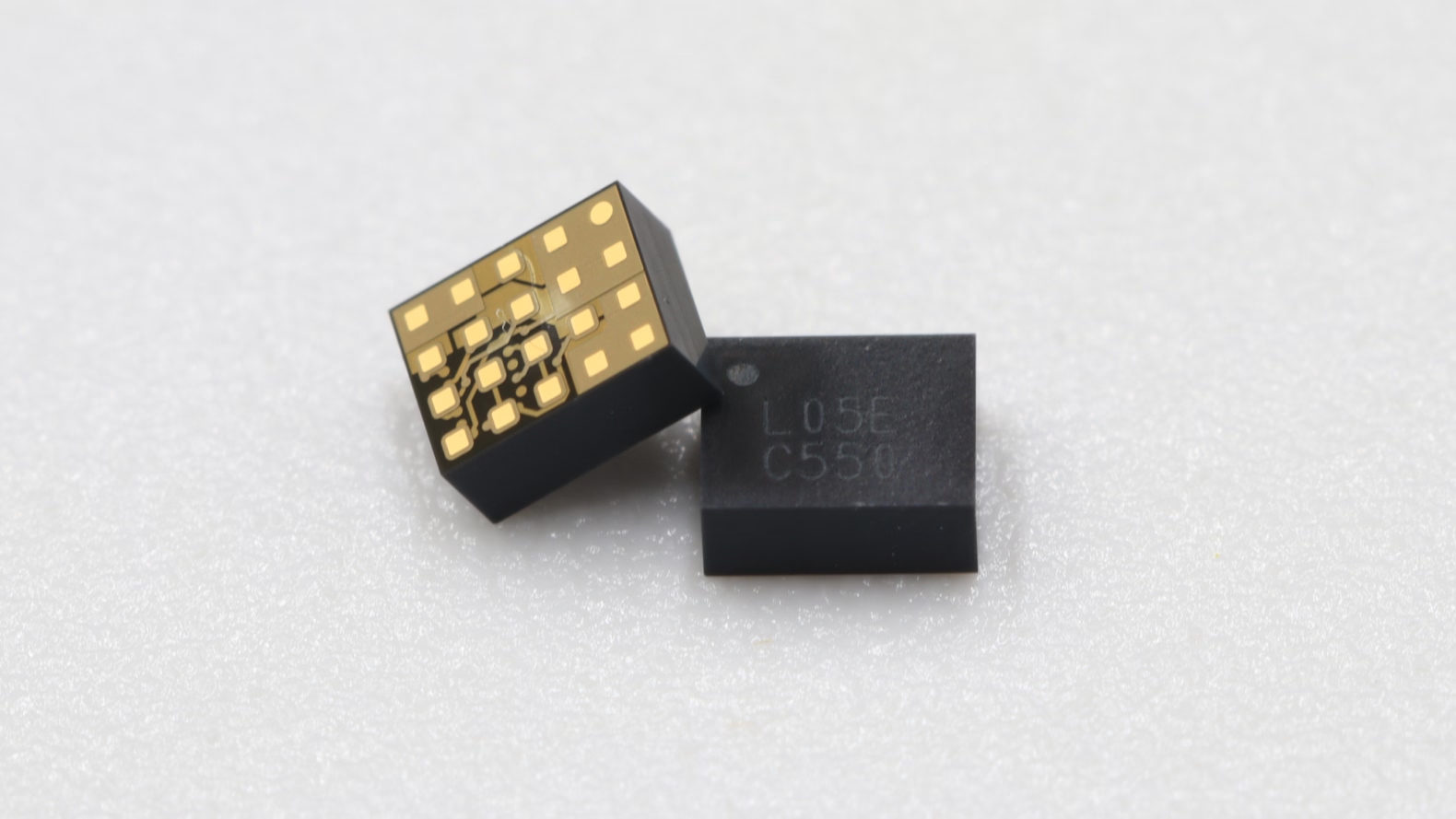
Miniaturizing a power supply introduces several challenges. Higher component density makes thermal management more demanding, while noise from the power converter can affect sensitive circuitry elsewhere in the system.
The LBK0504 solves both issues simultaneously: it can deliver up to 4 A of continuous output current while keeping thermal dissipation low and suppressing noise by combining up to 95% efficiency with a high switching frequency and 70 dB PSRR. It can switch at its nominal 6 MHz frequency, or it can be externally synchronized in the range from 4 MHz to 8 MHz. It supports input voltage levels from 2.3 V to 5.5 V and delivers a regulated output voltage in the range from 0.4 V to 4.9 V. For these reasons, it offers an efficient, flexible, and low-noise point-of-load solution for tight board layouts.
Power-supply noise is particularly relevant in systems containing high-speed communication, RF, sensing, or measurement circuitry. Unwanted noise on a supply rail can interfere with sensitive signals and affect overall system performance.
This noise can, for example, modulate RF synthesized clocks and sensitive optical TIA (transimpedance amplifier) inputs, induce phase jitter, close transceiver eye diagrams, and degrade precision ADC dynamic range.
Featuring 70 dB PSRR, the LBK0504 provides active input-rail rejection across the power distribution network (PDN), suppressing switching harmonics before they propagate downstream. This enables direct powering of noise-sensitive signal paths and eliminates the need for secondary LDO post-regulators and discrete LC filters with the overhead related to their footprint, insertion loss, and thermal management.
For high-current core rails exceeding the maximum output current of a single device, multi-phase configurations exist, where up to four LBK0504 devices can be configured in parallel to deliver up to 16 A continuous output.
Phase-interleaved operation multiplies the effective switching frequency, which significantly suppresses input and output RMS ripple current and improves dynamic load transient response. This can be particularly beneficial for dense SoCs and FPGAs. Additionally, distributing power conversion across multiple units optimizes PCB thermal spreading and eliminates the risk of localized hotspots without requiring larger, higher-profile inductor footprints.
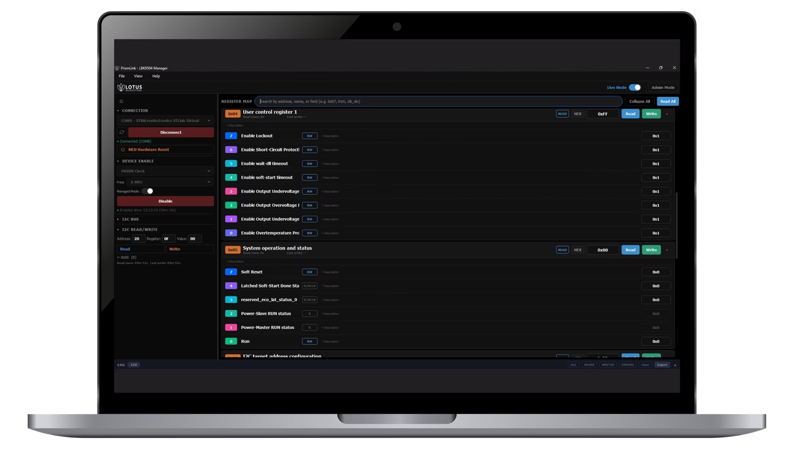
The onboard I²C interface can communicate with the Lotus LMS PRISM Console to streamline device evaluation and system validation. Engineers can easily configure all the details of the operation of the LBK0504, like defining custom register presets, setting soft-start ramp rates, adjusting bus timeouts, and managing slave addressing.
To support active debugging, the console enables direct power-on control and real-time Power Good (PG) monitoring. Ensuring hardware safety is equally straightforward: designers can selectively activate or deactivate the integrated fault-protection suite—including UVLO, OTP, OVP/UVP, and cycle-by-cycle current limiting—without altering external hardware.
By combining integrated power conversion, low-noise performance, digital configurability, and multi-phase scalability, the LBK0504 provides a flexible approach to power delivery as system requirements continue to increase.
Engineering samples and evaluation boards are available via the Lotus Microsystems Early Access Program. Register to start testing the LBK0504 in your next design.


